Semiconductors are everywhere in our daily lives, even though we hardly ever get to see them. They are concealed in all our technical devices, from hairdryers to satellites. In this interview, Holger Krumme, Managing Director of HTV Halbleiter-Test & Vertriebs-GmbH and HTV Conservation GmbH, offers some insights into this hidden world.


Managing Director Holger Krumme is proud of the services offered by HTV, one of the very few companies in the world that can conserve electronic components for up to 50 years in a highly secure warehouse.
Mr. Krumme, in February 2023, the TÜV NORD GROUP acquired a majority holding in the HTV Group through its tech subsidiary, ALTER. What kind of role does HTV play in the world of semiconductors?
Semiconductors are the fundamental building block in microchips, the little black boards with lots of metal pins that you find on all printed circuit boards. They are the basis of our connected world. Without them, we wouldn’t be able to make phone calls or drive our cars. We wouldn’t even have electricity: Huge numbers of microchips are installed in every wind turbine and every coal-fired power plant. Our job at HTV is to ensure that our customers, who come from sectors including the automotive industry, medical technology and industry in general, only process chips of the very highest quality. It’s especially crucial in these sectors for these products to function as reliably as possible for as long as possible.
With what issues do your customers come to you?
36 years ago, we started testing electronic components and assemblies, principally for industrial applications. Not every part that you get from an electronics dealer is of the same quality. We take responsibility for selection, which means that we test every component and only pass on those products to our customers that satisfy their quality requirements.
We also program components. A microchip has no inherent function; you can use the same chip to adjust the rear-view mirror in your car or wind the windows up or down. It all depends on the programming. The carmaker sends us the relevant software, and we transfer it onto the chips: This is known as “flashing”.
Customers also bring defective components and assemblies for us to find out the cause of the problem. We have our own accredited institute for material analysis for this purpose. When it comes to material fractures, we start off with a light microscope to assess the surface. We can then use a scanning electron microscope to bring even more details to light, and our metallographic analysis offers insights into the inner structure of the materials.


How was the semiconductor crisis of 2020 to 2022 for you?
Whenever a product becomes scarce and its price goes up forgers try to cash in by making copies. This was also the case with microchips. During this time our customers had to contend with a lot of fakes, and we were frequently called upon to verify whether a supplied product really had been made by the stated manufacturer. The forgers are constantly refining their methods, which means that it’s becoming increasingly difficult to spot fakes. Here’s an example: If the writing on a chip can be wiped off with solvent, this will be indicative of a forgery, because the original data are etched on with a laser, making them indelible. With more recent forgeries, this wipe test is no longer fit for purpose, because the writing is embedded in additional layers that are impervious to solvent. What we do here is to make the deepest layer visible using an ultrasound method. But we also open every component to verify that what’s going on inside is consistent with the labelling.
Did the shortage of semiconductors have a knock-on effect on other business fields?
Yes, demand is increasing, even for long-term storage purposes. During the shortage, anyone wanting to get hold of high-quality chips would stockpile them to avoid future restocking issues. While lead times may since have normalised, the storage issue remains a hot potato, because chip manufacturers are constantly faced with the problem of no longer being able to make their products. If a chip series drops out of the range, our customers are faced with two options: They must either rework their product to adapt it to the new range or buy in so much material that their original product version can survive and enough replacement parts will be available. Medical technology products in particular have a very long life and need carefully certified assemblies. This means, of course, that the manufacturers would rather overhaul them to avoid having to recertify, so they prefer instead to stock up on parts.


An expert uses an acoustic microscope to examine a printed circuit board. The method is non-destructive, so the board can be reused.
“We relieve our customers of all anxiety related to theft, fire and natural disasters at a stroke.”
Holger Krumme, Managing Director of HTV Halbleiter-Test & Vertriebs-GmbH and HTV Conservation GmbH
Why do companies get you to conserve components instead of storing them themselves?
You can’t just put newly produced semiconductors on a shelf and pick them up later for further processing. If a microchip is not installed within one to two years, the contacts can oxidise, preventing the current from flowing. The blobs of solder and plastics emit plasticisers and solvents in gaseous form, and the structure of the carrier materials changes. We’ve developed a method that prevents corrosion and stops the ageing process. With thermic absorptive gassing (TAB®), we pack the components in bags with a special coating, fill them with a complex mix of gases and add absorber material which is exactly tailored to the materials. This allows us to set the oxygen and air humidity levels in the packet to the optimal values. We keep the packets in cold stores in our high-security building. This is made of solid armoured concrete and monitored by elaborate alarm and camera technology. Not only that, but the atmosphere in the storerooms is precisely calibrated to preclude the possibility of fire. In other words, we relieve our customers of all anxiety related to theft, fire and natural disasters at a stroke.
We check the stored components at regular intervals. This means that we run electric current through them at least once a year and test whether they are still working. This enables electrolytic capacitors to maintain their electrical properties. The low temperatures prevent the electrolytes from evaporating. This allows us to offer guaranteed storage periods of up to 50 years. As far as I know, this service is unique globally, which is why we have customers from all over, including Eastern Europe and Hong Kong.


In the case of components of dubious origin, an X-ray examination reveals whether the component even contains a chip.


It also shows up breakages among the very finest connecting wires.
What do you think about the plans to get more chip manufacturers to set up in Europe and Germany?
The pandemic and the semiconductor crisis have made it crystal clear how important it is for the German and European economies to wean themselves off their dependence on Asian manufacturers. The goal of setting up more production sites in Germany by 2030 is an ambitious one. Even if it takes longer, it’s going to be critical to start off this wave of new providers, which will gradually develop into an ecosystem. You can already see this happening in the Silicon Saxony area around Dresden.
And it goes without saying that building up production capacity will bring benefits for the HTV Group. As an experienced provider for testing and process development, we’ll be able to get on board as soon as the new market takes off. We’re planning to develop new capacities for packaging; this is the process in which semiconductors are given their black casings and fitted with connections pins. The semiconductor manufacturers don’t do this themselves; they pass this work on to service providers. Because we’re part of ALTER, we’re one of the few companies in Europe to have access to this expertise.


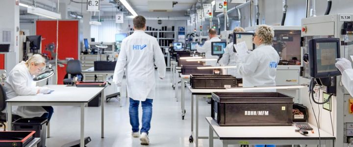
The HTV team uses state-of-the-art, fully automated large-scale testing systems to test hundreds of thousands of parts each day.
How is the takeover by the TÜV NORD GROUP impacting your work?
We’ve enjoyed the cooperation very much since the start and see a lot of opportunities for synergies. The TÜV NORD GROUP is very strong in aerospace technology, which is giving us access to a whole new industry. Assemblies installed in satellites, for example, have to function for a long time under extremely hard conditions. They must be able to withstand vacuum conditions, cosmic radiation and huge fluctuations in temperature.
For our part, we’re bringing in skills that aren’t yet so well established in the TÜV NORD GROUP. For space travel, you tend to work with lower production volumes. We can offer automatic handling systems for the testing and processing of large-scale batches that the automotive sector requires, for instance; our services also include programming and long-term storage.
The conditions for space research are very good in Germany. Which is why we’re so delighted to be able to complement our own expertise with that of the TÜV NORD GROUP. This will allow us to work together in the future to develop a shared field of research.